In the 21st century, many principles, theories, and various bodies of knowledge have been formulated leading to advanced technological development for more human convenient living. One technology apparently taking as a part in human life is nanotechnology. The nanotechnology is a technology occurred from applying multidisciplinary knowledge from many fields such as physics, chemistry, engineering, or applied science to make and synthesize atomic and molecular materials, also nanoscale parts and structures. Nanotechnology is utilized to develop materials or tools with specific physical, chemical, and biological properties or functions in response to human’s need in term of more life safety and convenience.
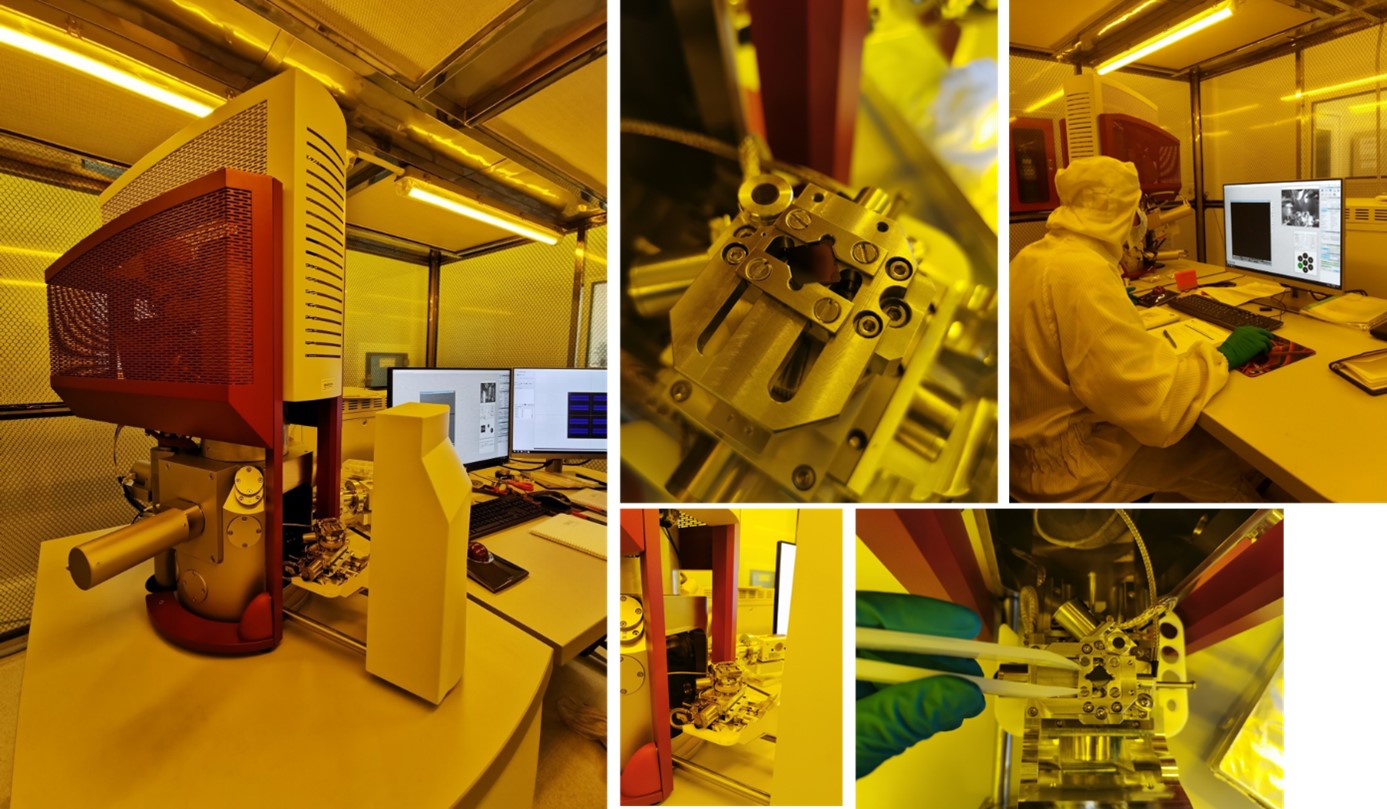
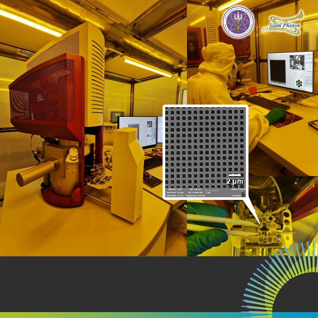
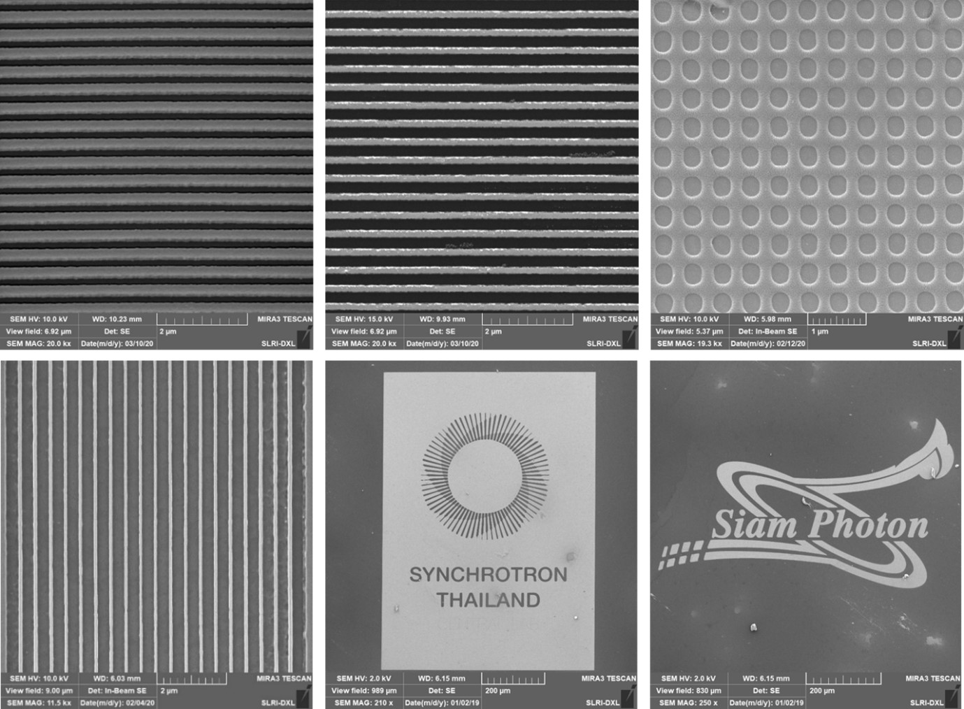
Microsystems Electronics and Control Systems (MEMs) laboratory at Beamline 6: Deep X-ray Lithography, Synchrotron Light Research Institute, the laboratory equipped with tools and instruments for production of nanoscale parts and structures, is upgraded in efficacy to support the era of nanotechnology. The FE-SEM (MIRA3 model) was installed to fabricate nanoscale-structure using Electron Beam Lithography (EBL) process. In this process, the focused electron beam is applied to create nanostructures on photoresist. The photoresist reacts to electrons and is rinsed off by Developer liquid to acquire nanoscale structure for adding metal on substrate and building metallic nanostructure later on.
The MEMs lab is currently developed and can make the small metallic structure at 100-nanometer scale with the Electron Beam Lithography to support frontier research and advanced technology.
Article by: Mr. Kiattisuk Srisoam, Laboratory Scientist
Dr. Pattanaphong Janphuang, Beamline Manager

111 SirinthonWitchothai Building, University Avenue, Muang District, Nakhon Ratchasima 30000, THAILAND
Tel.: +66 44 217 040 Fax: +66 44 217 047 Email: siampl@slri.or.th
Copyright © 2015 Synchrotron light research institute. All Rights Reserved.
|
|