




ภาพรวมระบบลำเลียงแสงและสถานีทดลอง
Beamlines & Experimental Stations
A beamline is a system of components, such as slits, monochromators, focusing mirrors, and other optical elements used for shaping and delivering the synchrotron light from the storage ring to the experimental stations. An experimental station, located at the end of a beamline, contains measurement systems for a specific measurement technique. The SLRI beamline currently has 11 beamlines with 12 experimental stations in routine operation.
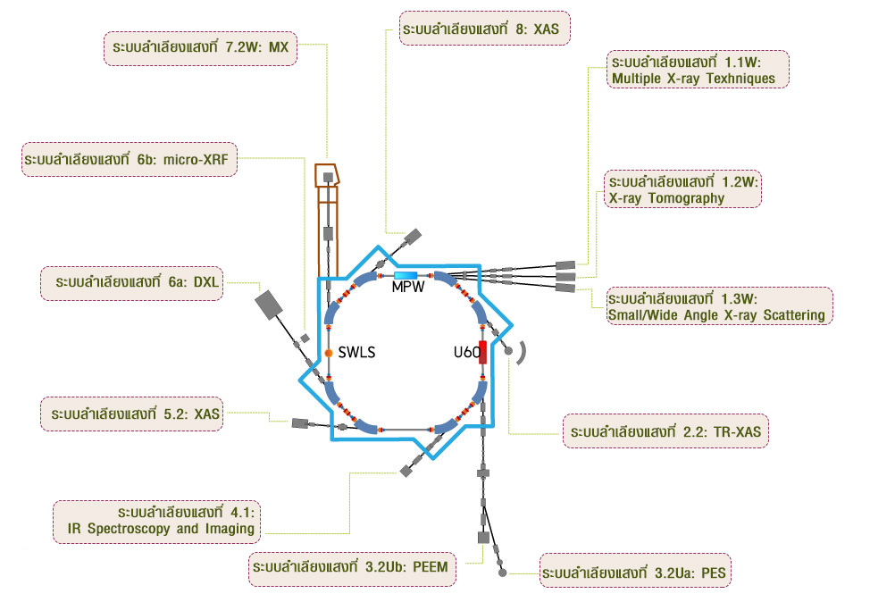
Beamline Map
Beamlines branching off the SPS electron storage ringClick a beamline label (BL) on the map to see its techniques and station website
Beamline List
12 experimental stations · Click a station for detailsAdvanced Techniques at SLRI
Powerful methods for science and technology · Click a card for technique details and available stationsSpectroscopy19 techniques
Investigates local atomic structure and electronic states by analyzing X-ray absorption patterns.
View details and stationsCaptures dynamic changes in electronic and structural properties over time.
View details and stationsCombines XAS with micro-focused beams for localized structural analysis.
View details and stationsSurface-sensitive absorption spectroscopy for thin films and interfaces.
View details and stationsDetermines elemental composition by detecting characteristic X-ray emissions.
View details and stationsUltra-trace elemental analysis using total reflection geometry with very low detection limits.
View details and stationsIdentifies chemical bonds and functional groups using infrared absorption spectra.
View details and stationsAnalyzes electronic structure by detecting photoelectrons.
View details and stationsQuantifies elemental composition and chemical states within the top nanometers via core-level photoemission.
View details and stationsDepth-sensitive XPS using emission angle to separate surface and near-surface information and probe anisotropy.
View details and stationsStudies electronic structure by measuring photoelectrons emitted from a sample.
View details and stationsProbes electronic band structure by measuring photoelectrons emitted at different angles.
View details and stationsStudying orientation-dependent absorption.
View details and stationsNear-edge region of XAS sensitive to bonding, functional groups, and molecular orientation.
View details and stationsSpatially resolved XPS providing micron-scale chemical state mapping for surfaces.
View details and stationsProbes the electronic band structure with high spatial resolution, enabling microscale analysis.
View details and stationsElectron Energy Loss Spectroscopy at microscopic scale to probe electronic structure and chemical composition.
View details and stationsHigh-resolution NEXAFS imaging for mapping molecular orientation and bonding.
View details and stationsNEXAFS detected via Auger yield with micron spatial resolution for chemical state mapping.
View details and stationsDiffraction7 techniques
Identifies crystalline phases in powdered samples by analyzing diffraction patterns.
View details and stationsA cutting-edge method for probing site-specific atomic arrangements and subtle structural variations in complex materials.
View details and stationsDetermines 3D structures of macromolecules by analyzing X-ray diffraction patterns from crystals.
View details and stationsDetermines residual stress in materials by measuring diffraction at different tilt angles.
View details and stationsSurface diffraction technique using low-energy electrons to determine atomic structure and surface symmetry.
View details and stationsLocalized LEED analysis with micrometer-scale resolution for studying specific surface regions and defects.
View details and stationsQuantitative surface diffraction technique analyzing LEED intensity as a function of electron energy to determine atomic structure of surfaces.
View details and stationsScattering4 techniques
Characterizes nanoscale structures and particle size distributions.
View details and stationsCharacterizes crystalline order and structural motifs at shorter length scales.
View details and stationsSurface-sensitive scattering technique for thin films and nanostructures.
View details and stationsDetermines thickness, density, and roughness of thin films by analyzing reflected X-rays.
View details and stationsMicroscopy3 techniques
Full-field electron microscopy technique using photoemission to visualize surface morphology, electronic structure, and chemical contrast at the nanoscale.
View details and stationsReal-time, surface-sensitive imaging using elastically backscattered low-energy electrons to visualize phases, domains, and reconstructions.
View details and stationsAcquires intensity–voltage (I–V) curves of diffracted electron beams to determine surface atomic structure with high precision.
View details and stationsImaging7 techniques
Non-destructive technique for elemental analysis and mapping using focused X-rays at micrometer-scale resolution.
View details and stationsMaps elemental distribution in a sample using X-ray fluorescence over a wide field.
View details and stations3D imaging technique using X-rays to reconstruct internal structures with micrometer resolution.
View details and stationsUses X-rays to create two-dimensional images of internal structures with high resolution.
View details and stationsVisualizes chemical bonding and molecular orientation at surfaces using NEXAFS imaging.
View details and stationsChemical-state mapping over fields of view using scanning or full-field XPS detection.
View details and stationsFull-field photoemission imaging to spatially resolve work-function and electronic contrast at the nanoscale.
View details and stationsLithography1 technique
A microfabrication method using high-energy X-rays to produce high-aspect-ratio structures for MEMS and microfluidics.
View details and stationsSupport Facilities & Equipment
Siam Photon Laboratory (SPL) has prepared a range of advanced instruments and facilities to support usersBasic tools for sample preparation
- Pestle and mortar
- Tweezers
- Spatulas, etc.
Readability: 0.01 g
- Built-in glass draft shield for high weighing stability.
- Applications: general laboratory use, formulation, and quality control where 0.01 g precision is required.
Readability: 0.1 mg (0.0001 g)
- Built-in glass draft shield for high weighing stability.
- Applications: high-precision weighing for analytical chemistry, sample preparation, and pharmaceutical research.
Chemical fume hood
- Work area: 1200 mm (W) × 800 mm (D) × 1200 mm (H)
- Airflow velocity: 0.5 m/s (average face velocity at sash opening)
- LED lighting, ≥ 800 lux inside work area
Pressing pellets
- Maximum force: 15 US tons (13.6 metric tons)
- Evacuable pellet die diameters: 6, 10, 13, 16 and 20 mm
- Each die set has a maximum force rating that should not be exceeded — check the front of the die for the maximum load capacity.
Controlled heating for lab processes
- Volume: 53 liters (1.9 cu. ft.)
- Working temp. range: ambient +10 °C to +300 °C
- Temperature accuracy: 0.1 °C up to 99.9 °C, 0.5 °C from 100 °C
- Adjustable temperature, fan speed, air flap position and program time
Extremely fast grinding of very small samples in a single step
- Adjustable from 900 to 3,000 oscillations/min (15–50 Hz)
- Max feed size 6 mm · final fineness down to 5 µm
- Sample quantity 0.1 – 5 ml
- Bowls 5, 10, 15 ml · balls 0.1 – 15 mm · zirconium oxide, stainless steel, PTFE
How to Apply for Beamtime
Steps for requesting synchrotron beamtime, for academic institutions and government agenciesBeamtime Submission ProcessProcedure for SLRI Beamtime Request for Educational Institute and Government Sector
- 1Consultation
Beamline Scientists / User Service Section offers advice to applicants on making beamtime proposals.
- 2Submit proposal
Applicants submit proposals via the Beamtime Application System (BeamApp) https://user.slri.or.th in request for beamtime.
- 3Proposal review
Committees review the submitted proposals at least 14 days.
≥ 14 days - 4Beamtime allocation
Beamline Operation Section allocates beamtime within 15 days, and User Service Section informs the allocation schedule to applicants 14 days before beamtime service.
within 15 daysnotified 14 days before - 5Confirm beamtime & participants
Each applicant confirms the beamtime via the email at userservice@slri.or.th and submits the name list of all members conducting experiments at SLRI via BeamApp at least 3 days (domestic users) and 7 days (overseas users) before the beamtime date.
domestic ≥ 3 daysoverseas ≥ 7 days - 6Online safety training
All new users must complete and pass the Online Safety Training for SLRI users at least three days before arriving at SLRI for the beamtime project.
≥ 3 days before arrival - 7On arrival
Upon arrival, users get a radiation dosimeter, a radiation record form, and an SPL access card before doing the experiment.
- 8After the experiment
Each user returns the dosimeter, the completed form, and the access card to a security guard, and submits the questionnaire and End-of-run report via online platforms.
report within 14 days
Using BeamApp step by stepSummary of the Beamtime Application System Manual · Click a topic for details
1Log in / Register / Forgot password
- Enter BeamApp at https://user.slri.or.th/.
- Existing users: fill in your Username and Password to log in.
- New users: click “Register a new membership”, then fill in “Personal Information” and “Other Information”.
- Forgot password: click “I forgot my password” and enter the e-mail you registered with to receive a new password.
2Beamtime Application
- Click “Apply for beamtime”, read the “Terms & Policies”, select “I agree to the Terms & Policies” and click “Submit”. (If you select “Cancel”, the project cannot be submitted.)
- User Information: your details, the Principal Investigator (P.I.) — if you are a student the P.I. must be your supervisor (“Select new P.I.”), a request for a Confirmation Letter of Beamtime Allocation if needed, and “Internal Project” for SLRI scientists.
- Participants: click “Add Participant” (only users registered in BeamApp can be selected — new users must register first) and “Add SLRI collaborator” if an SLRI scientist will be your local contact. Use “Search” by name / surname / e-mail, then “Select”.
- General Information:
- Sample: complete the sample list with all relevant information and techniques based on the General Information.
- Specific Information: complete the technique-specific form for the technique you selected (e.g. XAS).
- Preview: review all project information, then click “Submit proposal to SLRI”. Submitted projects are listed under “Submitted Project(s)”.
- Students: the P.I. (advisor) must approve the project — under “Waiting for P.I. Approval”, click “Action”, edit with “Previous” if needed, then “Submit proposal to SLRI”.
3Beamtime Allocation
- The P.I. and all participants listed in the project receive a beamtime allocation e-mail.
- Check the schedule in BeamApp: “Submitted Project(s)” → click the icon in the “Action” column of the project to display the allocated beamtime.
- To get a Synchrotron Beamtime Allocation Results Letter: “Allocated Project(s)” → open the project → click the download icon for the e-Document.
4Experimental Feedback Requirements
To help us improve our services, the Institute requests all synchrotron users to provide the following documents after completing their beamtimes:
Complete the post-experiment satisfaction evaluation through the BeamApp system once your experiment has concluded.
Experimental Report — submit a summary report of your experimental results within 14 days after the completion of your experiment via BeamApp.
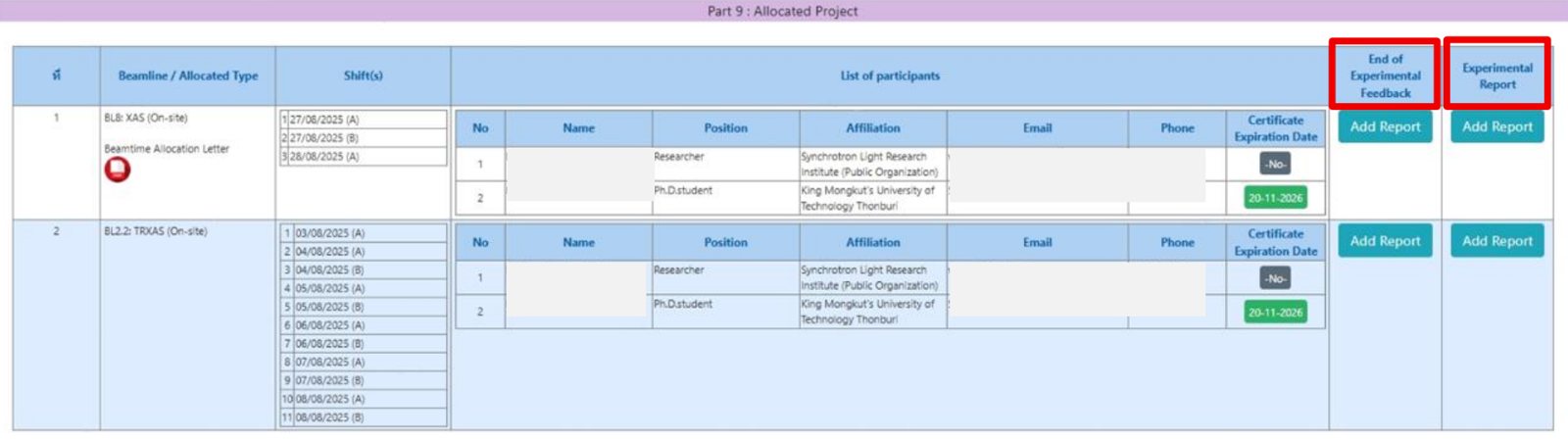 BeamApp → Part 9: Allocated Project → click “Add Report” in the End of Experimental Feedback and Experimental Report columns
Estimate Your Beamline Shifts1 shift = 11 hours
To view detailed information about shift estimation, please return to the homepage of the beamline you are interested in. Each beamline provides its own specific guidelines and data for calculating shifts.
Safety Guidelines for Beamline Operation
To ensure safe and compliant beamline operations, all users must strictly follow the established safety protocols.1. Training & Authorization
- Only authorized personnel are permitted to operate or control the beamline equipment.
- All users must complete the Beamline Hutch Search and Secure training, as well as radiation safety procedures, before operating any beamline system.
- Users are also required to sign the form in Appendix 4: Beamline Safety Training.
 Example of Appendix 4 — Beamline Safety Training form for user signatures (click to enlarge)
- Appendix 1Safety manual for beamline local contact — local contact has read and understood the safety manual
- Appendix 2User checklist before proceeding the experiment by local contact — users have been successfully verified
- Appendix 3Beamline security check — safety systems of the beamline are ready for operation
- Appendix 4Beamline safety training — all users have been instructed and sign with name and signature
- Appendix 5Beamline checklist after proceeding the experiment by local contact
2. Radiation Safety Requirements
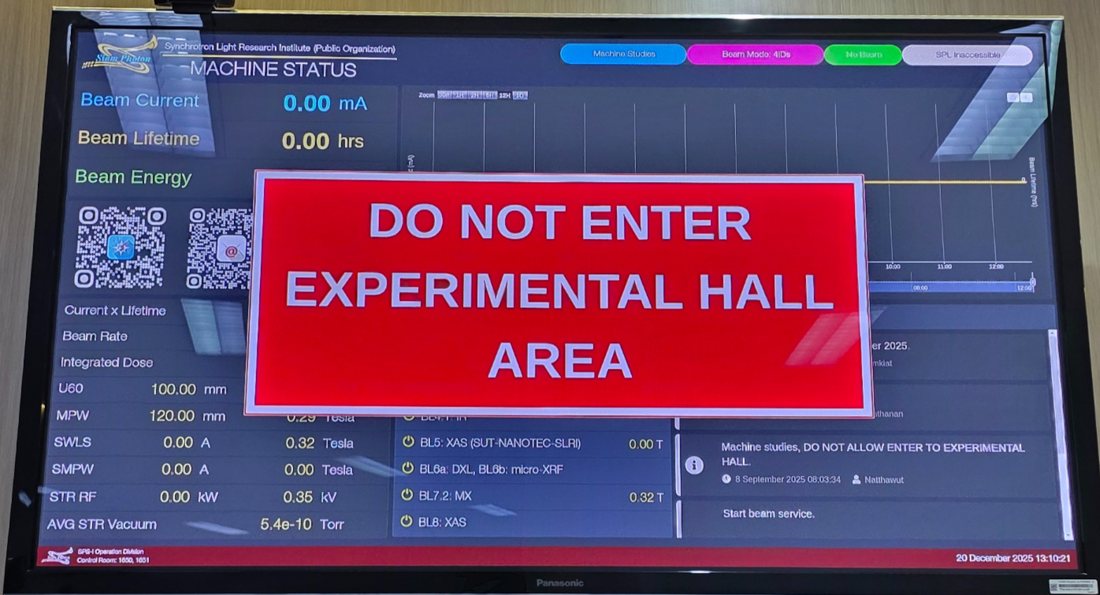
Users are not allowed to remain in the experimental hall during beam injection under any circumstances.
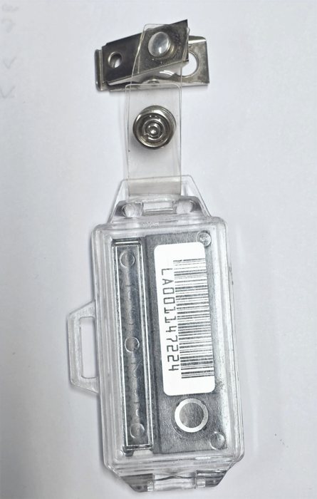
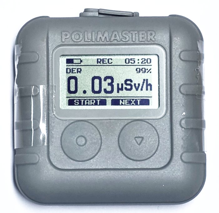
A radiation monitoring badge must be worn at all times while inside the experimental hall.
3. Conduct in the Experimental Area
Food and beverages are strictly prohibited at the beamline area.
Users are responsible for cleaning and tidying the beamline area on the final day of their scheduled beamtime.
Users must take back their samples, chemicals, and any chemical waste generated during experiments.
Publications
Explore published research outputs by fiscal year through an interactive Power BI dashboard.Multiple X-ray Techniques
MXT · Established 2016
X-ray Imaging & Microtomography
XTM · Established 2016
Small & Wide-Angle X-ray Scattering
SAXS/WAXS · Established 2011
Time-resolved X-ray Absorption Spectroscopy
TRXAS · Established 2011
Photoelectron Emission Spectroscopy
PES · Established 2003
Photoemission Electron Microscopy
PEEM · Established 2011
Service Techniques
micro-Infrared Spectroscopy & Imaging
µIR · Established 2010
X-ray Absorption Spectroscopy (ASEAN Beamline)
ASEAN BL · Established 2026
X-ray Absorption Spectroscopy (SUT-NANOTEC-SLRI)
XAS · Established 2013
Deep X-ray Lithography
DXL · Established 2006
Macromolecular Crystallography
MX · Established 2009
Service Techniques
X-ray Absorption Spectroscopy / X-ray Fluorescence Imaging
XAS/XFI · Established 2005
X-ray Absorption Spectroscopy
Spectroscopy · Available at 6 stations
X-ray Absorption Spectroscopy (XAS) is a synchrotron-based analytical technique used to investigate the electronic and local atomic structures of materials with element-specific precision. By measuring the absorption of X-rays as a function of photon energy across the absorption edge of a target element, XAS provides two key types of structural information:
- X-ray Absorption Near Edge Structure (XANES) – which reveals oxidation states, chemical environments, and electronic configurations; and
- Extended X-ray Absorption Fine Structure (EXAFS) – which identifies coordination numbers, interatomic distances, and the geometric arrangement surrounding the absorbing atom.
Benefits of Synchrotron Techniques
Synchrotron XAS offers high brightness and tunable energy, enabling precise measurements of XANES and EXAFS regions for detailed chemical and structural analysis.
Applications
Used for oxidation state analysis, coordination environment studies, and chemical bonding investigations in catalysts, nanomaterials, and thin films.
Relevant beamline (s)Experimental stations offering this technique
Time-resolved X-ray Absorption Spectroscopy
Spectroscopy · Available at 1 station
Time resolved X-ray Absorption Spectroscopy (TRXAS) measures the X-ray absorption coefficient at specific energy levels over extremely short time intervals. Capturing spectra in the pico- to millisecond range, it allows researchers to track the evolution of local electronic and geometric structures. It is essential for observing transient intermediate states in rapid chemical reactions.
Benefits of Synchrotron Techniques
Captures transient intermediate states and rapid structural changes that are invisible in steady-state measurements.
Applications
Studying fast catalytic reactions, battery charge/discharge cycles, and photochemical reactions.
Relevant beamline (s)Experimental stations offering this technique
Micro X-ray Absorption Spectroscopy
Spectroscopy · Available at 1 station
Micro-XAS: This method utilizes sophisticated X-ray optics to focus the beam down to a micrometer scale. It performs X-ray Absorption Spectroscopy on tiny, specific spots within a heterogeneous sample to determine local oxidation states and coordination chemistry. This provides high spatial resolution for complex materials.
Benefits of Synchrotron Techniques
Provides local chemical and structural information (oxidation state, coordination) with high spatial resolution.
Applications
Geology (mineral inclusions), biological tissues (metal distribution in cells), and complex environmental samples.
Relevant beamline (s)Experimental stations offering this technique
Grazing-Incidence X-ray Absorption Spectroscopy
Spectroscopy · Available at 2 stations
GIXAS: X-rays are directed at the sample at a very shallow, “grazing” angle near the critical angle for total reflection. This geometry limits the penetration depth of the X-rays, making the technique exceptionally sensitive to the surface and thin-film layers. It minimizes background noise from the bulk substrate.
Benefits of Synchrotron Techniques
Enhances surface sensitivity, allowing the study of thin films and interfaces by minimizing background signal from the substrate.
Applications
Investigating surface oxidation, interface reactions in electronics, and ultra-thin coatings.
Relevant beamline (s)Experimental stations offering this technique
X-ray Fluorescence
Spectroscopy · Available at 6 stations
X-ray Fluorescence (XRF) is based on the interaction between high-energy X-rays and the atoms in a sample. When the sample is irradiated with primary X-rays, inner-shell electrons are ejected, creating vacancies. Electrons from higher energy levels then fill these vacancies, releasing secondary X-rays (fluorescent X-rays) with energies characteristic of each element. By detecting and analyzing these emitted X-rays, XRF provides qualitative and quantitative elemental composition without destroying the sample.
Benefits of Synchrotron Techniques
Synchrotron-based XRF offers exceptional sensitivity and spatial resolution compared to conventional XRF. The intense and highly collimated synchrotron X-ray beam enables detection of trace elements at very low concentrations, precise quantitative analysis, and micro-scale elemental mapping. It is ideal for studying complex, heterogeneous materials without sample destruction.
Applications
XRF is widely applied in material science, geology, environmental monitoring, and cultural heritage studies. It is used for elemental analysis of metals, ceramics, polymers, soils, and biological samples. Synchrotron XRF enables micro-scale mapping for advanced research in nanomaterials, thin films, and contamination analysis.
Relevant beamline (s)Experimental stations offering this technique
Total Reflection X-ray Fluorescence
Spectroscopy · Available at 1 station
TXRF is based on the excitation of atoms by an incident X-ray beam under total reflection conditions at very small angles. This geometry minimizes background scattering and enhances the detection of fluorescence signals from trace elements. The emitted characteristic X-rays are analyzed to determine elemental composition. Because the penetration depth is extremely shallow, the technique is highly surface-sensitive.
Benefits of Synchrotron Techniques
Provides higher brightness and improved sensitivity for ultra-trace detection. Enables better signal-to-noise ratios and element-selective analysis through tunable X-ray energy.
Applications
Used for trace element analysis, surface contamination monitoring, and quality control in semiconductors. Also applied in environmental, biological, and material analysis.
Relevant beamline (s)Experimental stations offering this technique
Fourier-Transform Infrared Spectroscopy
Spectroscopy · Available at 1 station
Synchrotron-based Fourier transform infrared (SR-mFTIR) microspectroscopy redefines the limits of chemical mapping by coupling the analytical power of infrared spectroscopy with the extreme brilliance of synchrotron light. Unlike conventional thermal sources, synchrotron radiation provides a highly collimated photon beam effectively 1,000 times brighter than a standard instrument.
This capability allows researchers to focus light onto microscopic samples with diffraction-limited spatial resolution while maintaining an exceptional Signal-to-Noise Ratio (SNR). The result is high-definition chemical mapping at the micrometer scale, revealing fundamental vibrational transitions and molecular fingerprints with unparalleled clarity.
Benefits of Synchrotron Techniques
Synchrotron IR is 100-1000x brighter than thermal sources, allowing for diffraction-limited spatial resolution in imaging.
Applications
Identifying chemical functional groups in polymers, drug-cell interactions, and micro-plastics.
Relevant beamline (s)Experimental stations offering this technique
Photoelectron Emission Spectroscopy
Spectroscopy · Available at 1 station
Photoelectron Emission Spectroscopy is based on the photoelectric effect, where incident photons with sufficient energy strike a material and cause the emission of electrons from its surface. The kinetic energy of these emitted electrons is measured to determine their binding energy within the material. This information provides insight into the electronic structure and chemical composition of the sample. PES is widely used to analyze surface chemistry and electronic states of atoms and molecules.
Benefits of Synchrotron Techniques
Provides high energy resolution and tunable photon energy for detailed electronic structure analysis. Enhances surface sensitivity and signal quality.
Applications
Used for studying electronic structure and surface properties. Applied in materials science, surface science, and electronic materials.
Relevant beamline (s)Experimental stations offering this technique
X-ray Photoelectron Spectroscopy
Spectroscopy · Available at 1 station
XPS: This is a specific form of PES that uses X-rays to eject core-level electrons from atoms within the top 1-10 nm of a surface. The energy of the ejected electrons is unique to each element and its chemical environment. This allows for precise identification of elemental composition and oxidation states.
Benefits of Synchrotron Techniques
Highly quantitative; determines elemental composition, empirical formulas, and chemical/oxidation states of surfaces.
Applications
Corrosion studies, polymer surface modifications, and thin film depth profiling.
Relevant beamline (s)Experimental stations offering this technique
Angle-Resolved X-ray Photoelectron Spectroscopy
Spectroscopy · Available at 1 station
ARXPS: By varying the emission angle at which photoelectrons are detected, this technique changes the effective depth being probed. Steeper angles provide information from deeper layers, while shallow angles focus on the extreme surface. It enables non-destructive depth profiling of ultra-thin films.
Benefits of Synchrotron Techniques
Enables non-destructive depth profiling with improved resolution and sensitivity. Allows detailed analysis of layered structures.
Applications
Used for depth-dependent chemical analysis and thin film studies. Applied in coatings, semiconductors, and multilayer materials.
Relevant beamline (s)Experimental stations offering this technique
Ultraviolet Photoelectron Spectroscopy
Spectroscopy · Available at 1 station
UPS: This technique utilizes ultraviolet light to eject electrons specifically from the valence bands and molecular orbitals. Because UV photons have lower energy than X-rays, the kinetic energy of the ejected electrons provides detailed information about the highest occupied electronic states. It is primarily for measuring work functions and band alignments.
Benefits of Synchrotron Techniques
Provides high energy resolution and sensitivity to valence electronic states. Enables accurate measurement of work function and electronic structure.
Applications
Used for studying valence bands and surface electronic properties. Applied in semiconductors, organic electronics, and thin films.
Relevant beamline (s)Experimental stations offering this technique
Angle-Resolved Photoemission Spectroscopy
Spectroscopy · Available at 2 stations
ARPES: It measures both the kinetic energy and the emission angle (momentum) of photoelectrons ejected from a crystalline sample. Applying conservation laws directly maps the electronic band structure in momentum space. It is the most powerful tool for studying the electronic properties of quantum materials.
Benefits of Synchrotron Techniques
Delivers high energy and momentum resolution with tunable photon energy. Enables direct mapping of electronic band structures.
Applications
Used for studying band structure, Fermi surfaces, and electronic properties. Applied in superconductors, topological materials, and 2D materials.
Relevant beamline (s)Experimental stations offering this technique
Angle-resolved X-ray Absorption Spectroscopy
Spectroscopy · Available at 1 station
ARXAS: This technique measures X-ray absorption while changing the angle between the X-ray polarization vector and the sample’s orientation. Because X-ray absorption is highly directional, it reveals the preferential orientation of specific bonds. It is commonly used to study ordered molecular films and anisotropic crystals.
Benefits of Synchrotron Techniques
Determines the preferential orientation of molecular orbitals or bonds in anisotropic materials.
Applications
Studying molecular alignment in liquid crystals and anisotropic semiconductor crystals.
Relevant beamline (s)Experimental stations offering this technique
Near-Edge X-ray Absorption Fine Structure
Spectroscopy · Available at 1 station
NEXAFS: It involves measuring the X-ray absorption spectrum in the region near the absorption edge, typically within 50 eV of the threshold. This region is sensitive to the transition of core electrons to unoccupied molecular orbitals. It provides detailed information on local bonding environments and molecular orientations.
Benefits of Synchrotron Techniques
Sensitive to the local bonding environment, vacant orbitals, and molecular orientation.
Applications
Used for probing carbon bonding (sp² vs. sp³ hybridization), analyzing polymer orientation, and investigating soft-matter surfaces.
Relevant beamline (s)Experimental stations offering this technique
Micro X-ray Photoelectron Spectroscopy
Spectroscopy · Available at 1 station
Micro-XPS: A focused X-ray beam is used to perform photoelectron spectroscopy on a micrometer-scale spot. By raster-scanning the beam, the technique can map the chemical states of different elements across a surface. It is critical for analyzing the heterogeneity of microelectronic components and materials.
Benefits of Synchrotron Techniques
Provides high spatial resolution with enhanced chemical sensitivity. Enables localized surface composition analysis.
Applications
Used for microscale chemical mapping and defect analysis. Applied in microelectronics, nanomaterials, and surface studies.
Relevant beamline (s)Experimental stations offering this technique
Micro-Angle-Resolved Photoemission Spectroscopy
Spectroscopy · Available at 1 station
Micro-ARPES: This technique combines the momentum-resolved capabilities of ARPES with a micro-focused photon beam. It allows researchers to perform band structure mapping on micrometer-sized samples or specific domains. This is particularly useful for studying small flakes of 2D materials or heterogeneous surfaces.
Benefits of Synchrotron Techniques
Provides high spatial resolution combined with band structure mapping. Enables analysis of heterogeneous and microstructured materials.
Applications
Used for spatially resolved electronic structure studies. Applied in nanomaterials, microdevices, and complex materials systems.
Relevant beamline (s)Experimental stations offering this technique
Micro Electron Energy Loss Spectroscopy
Spectroscopy · Available at 1 station
Micro EELS: It measures the energy lost by an electron beam as it interacts with a sample, typically over a microscopic or nanoscopic area. The energy loss corresponds to electronic excitations, plasmons, or core-level transitions. It provides localized chemical and electronic information similar to XAS but with higher spatial resolution.
Benefits of Synchrotron Techniques
Provides high spatial resolution (micro/nano) for chemical and electronic analysis.
Applications
Mapping plasmons in nanoparticles and chemical states in thin films.
Relevant beamline (s)Experimental stations offering this technique
Micro Near-Edge X-ray Absorption Fine Structure
Spectroscopy · Available at 1 station
Micro-NEXAFS: A focused X-ray beam is used to probe near-edge absorption features at the micrometer scale. By scanning the beam across the sample, the technique maps the electronic structure and chemical bonding of specific elements in heterogeneous materials. It is essential for studying chemical variations at small spatial scales.
Benefits of Synchrotron Techniques
Provides element-specific information with high spatial resolution. Enables detailed analysis of electronic structure and chemical states.
Applications
Used for microscale chemical mapping and speciation analysis. Applied in polymers, nanomaterials, environmental samples, and biological systems.
Relevant beamline (s)Experimental stations offering this technique
Auger-yield Micro Near-Edge X-ray Absorption Fine Structure
Spectroscopy · Available at 1 station
Auger yield Micro NEXAFS: A focused X-ray beam is used to excite electrons, and Auger electron emission is detected to obtain near-edge absorption information. The technique provides surface-sensitive chemical analysis by collecting signals from the top few nanometers of the material. It is highly effective for investigating surface and interface properties.
Benefits of Synchrotron Techniques
Provides high surface sensitivity with enhanced chemical specificity. Enables precise analysis of surface electronic structure and bonding.
Applications
Used for surface chemical mapping and thin film analysis. Applied in coatings, catalysis, nanomaterials, and surface modification studies.
Relevant beamline (s)Experimental stations offering this technique
Powder X-ray Diffraction
Diffraction · Available at 1 station
Powder X-ray Diffraction (PXRD) is based on the diffraction of X-rays by the crystalline planes of a powdered sample. When X-rays interact with the sample, they are scattered at specific angles according to Bragg’s law, generating a characteristic diffraction pattern. This pattern reflects the crystal structure, phase composition, and lattice parameters of the material. By analyzing the positions and intensities of the diffraction peaks, detailed structural information can be obtained.
Benefits of Synchrotron Techniques
Provides high brightness, resolution, and sensitivity for rapid data collection and detection of subtle structural changes. Supports element-specific and in situ/operando studies through tunable X-ray energy.
Applications
Used for phase identification, quantification, and crystal structure analysis, as well as monitoring phase transitions. Applied in materials science, chemistry, pharmaceuticals, nanotechnology, and functional materials.
Relevant beamline (s)Experimental stations offering this technique
Anomalous X-ray Diffraction
Diffraction · Available at 1 station
Anomalous X-ray Diffraction (AXRD) utilizes the variation in atomic scattering factors near the absorption edge of specific elements. By tuning the X-ray energy close to the absorption edge, the scattering contribution of selected elements changes significantly. This enables element-specific structural analysis and enhances contrast between different atomic species. AXRD is particularly useful for distinguishing similar elements and investigating site occupancy and local structural environments.
Benefits of Synchrotron Techniques
Provides element-specific structural information through tunable X-ray energy. Enhances contrast and sensitivity for complex materials.
Applications
Used for phase identification, site occupancy analysis, and structural studies. Applied in catalysts, alloys, battery materials, and nanomaterials.
Relevant beamline (s)Experimental stations offering this technique
Macromolecular Crystallography
Diffraction · Available at 1 station
Macromolecular Crystallography (MX) technique enables the determination of the atomic structures of biomolecules. When a crystal containing macromolecules is hit by X-rays, the X-rays diffract in many directions, thus creating a unique diffraction recorded on a detector. The resulting X-ray data are mathematically processed to reconstruct an electron density map, thus revealing the precise 3D arrangement of atoms. This is essential for gaining biological insights and understanding the function of complex molecules.
Benefits of Synchrotron Techniques
Tunable wavelength is enabled for anomalous scattering in MX, thus targeting an element’s absorption edge and making it essential for modern biological structure solving.
Applications
Drug design and enzyme function
Relevant beamline (s)Experimental stations offering this technique
Residue Stress (Sin²Ψ method)
Diffraction · Available at 1 station
Residue Stress (Sin²Ψ method): This technique measures the change in the distance between atomic planes (d-spacing) as the sample is tilted at various angles (ψ). These shifts in the diffraction peaks indicate lattice strain caused by internal stresses. It provides a non-destructive way to calculate the residual stress within a material.
Benefits of Synchrotron Techniques
Provides high accuracy and sensitivity for stress measurements with improved peak resolution. Enables rapid, non-destructive analysis of internal strain using high-intensity X-rays.
Applications
Used for evaluating residual stress and strain in materials. Applied in metals, coatings, thin films, and engineering components.
Relevant beamline (s)Experimental stations offering this technique
Low-Energy Electron Diffraction
Diffraction · Available at 1 station
Low-Energy Electron Diffraction (LEED) uses low-energy electrons (typically 20–200 eV) incident on a crystalline surface to produce diffraction patterns. The diffracted electrons form characteristic spots that reflect the surface atomic arrangement. This allows determination of surface symmetry, periodicity, and reconstruction.
Benefits of Synchrotron Techniques
Synchrotron radiation enhances LEED studies by providing complementary high-resolution and element-sensitive measurements. It enables deeper insight into surface composition and electronic structure alongside diffraction data. The high brightness and tunability improve overall characterization accuracy.
Applications
LEED is used to determine surface crystallography, symmetry, and atomic ordering of materials. It is widely applied in surface science, thin film analysis, and semiconductor research. The technique is also essential for studying surface reconstructions and adsorption processes.
Relevant beamline (s)Experimental stations offering this technique
Micro Low-Energy Electron Diffraction
Diffraction · Available at 1 station
Micro-LEED: It uses a focused beam of low-energy electrons to produce a diffraction pattern from the topmost atomic layers of a surface. The micro-focus allows for the investigation of crystalline symmetry in small domains or individual grains. It is essential for verifying the quality of surface reconstructions.
Benefits of Synchrotron Techniques
Offers high spatial resolution with precise surface crystallography analysis. Enables localized diffraction studies on microstructured areas.
Applications
Used for determining surface structure and symmetry at small scales. Applied in nanostructures, thin films, and surface science.
Relevant beamline (s)Experimental stations offering this technique
Low-Energy Electron Diffraction – Intensity vs Voltage
Diffraction · Available at 1 station
LEED‑IV extends conventional LEED by measuring the intensity of diffracted electron beams as a function of incident electron energy (I–V curves). These energy-dependent intensity variations arise from multiple scattering interactions within the surface atomic layers. By comparing experimental I–V curves with theoretical simulations, precise atomic positions and surface relaxations can be determined. This approach provides quantitative structural information beyond symmetry analysis.
Benefits of Synchrotron Techniques
Although LEED uses electrons, synchrotron-based research environments enhance complementary surface studies through high precision, stability, and integration with other advanced characterization techniques. This allows comprehensive surface analysis combining diffraction with spectroscopy and imaging methods. The synergy improves data accuracy, reproducibility, and enables multi-modal investigation of complex materials.
Applications
LEED‑IV is widely used for determining surface atomic structures, including relaxations, reconstructions, and adsorption geometries. It is essential in catalysis research, semiconductor surface engineering, and thin film studies. The technique is also applied to investigate surface defects, alloy systems, and epitaxial growth processes.
Relevant beamline (s)Experimental stations offering this technique
Small-Angle X-ray Scattering
Scattering · Available at 1 station
Small-Angle X-ray Scattering (SAXS) is a technique that measures X-rays scattered at very small angles to investigate structures at larger length scales (typically 1–100 nm). It provides information about the size, shape, and distribution of nanoscale structures such as particles, pores, and macromolecules.
Benefits of Synchrotron Techniques
Provides high beam brightness, stability, and sensitivity for detecting weak scattering signals from nanoscale structures. Enables rapid data collection and high-resolution analysis of size, shape, and distribution. Supports in situ and time-resolved studies for monitoring dynamic processes in real time.
Applications
Used for characterization of nanoscale structures, including particle size, shape, and distribution, as well as pore structure and macromolecular organization. Applied in nanotechnology, soft matter, polymers, colloids, biological systems, and porous materials.
Relevant beamline (s)Experimental stations offering this technique
Wide-Angle X-ray Scattering
Scattering · Available at 3 stations
Wide-Angle X-ray Scattering (WAXS) measures X-rays scattered at large angles, corresponding to atomic-scale distances (0.1–1 nm). This technique reveals the degree of crystallinity, crystal size, and lattice parameters, and is widely applied in the study of polymers, nanocomposites, and other crystalline materials.
Benefits of Synchrotron Techniques
Provides high brightness, angular resolution, and sensitivity for precise analysis of atomic and crystalline structures. Enables rapid data acquisition and detection of subtle changes in lattice spacing and phase transitions. Supports in situ studies under tunable X-ray energies.
Applications
Used for crystal structure determination, phase identification and quantification, and analysis of crystallinity and molecular ordering. Applied in materials science, metallurgy, polymers, pharmaceuticals, and nanomaterials research.
Relevant beamline (s)Experimental stations offering this technique
Grazing Incidence Wide-Angle X-ray Scattering
Scattering · Available at 2 stations
GIWAXS: This technique combines the surface sensitivity of grazing incidence geometry with wide-angle scattering. By keeping the incident angle very low, the scattering signal comes predominantly from the thin-film surface rather than the substrate. It is ideal for studying the molecular packing and orientation in organic electronics.
Benefits of Synchrotron Techniques
Provides high surface sensitivity with enhanced resolution and fast data acquisition. Suitable for analyzing thin films and near-surface structures.
Applications
Used for studying crystalline structures and orientation in thin films. Applied in polymers, nanomaterials, coatings, and organic electronics.
Relevant beamline (s)Experimental stations offering this technique
X-ray Reflectivity
Scattering · Available at 1 station
XRR: X-rays are directed at a flat sample at very small grazing angles, and the reflected intensity is measured. The resulting interference patterns (Kiessig fringes) depend on the thickness, density, and roughness of the layers. It is a standard tool for characterizing thin films and multi-layer stacks.
Benefits of Synchrotron Techniques
Determines film thickness, surface/interface roughness, and electron density with sub-nanometer precision.
Applications
Quality control for semiconductor wafers and multi-layer optical coatings.
Relevant beamline (s)Experimental stations offering this technique
Photoemission Electron Microscopy
Microscopy · Available at 1 station
PEEM is based on the emission of electrons from a material’s surface when illuminated by ultraviolet or synchrotron radiation. The emitted photoelectrons are collected and magnified through an electron optics system to produce high-resolution surface images. The contrast arises from variations in work function, composition, and electronic structure.
Benefits of Synchrotron Techniques
Synchrotron radiation offers high brightness and tunable photon energy, enabling element-specific and chemical-state sensitivity. It enhances image contrast and allows detailed mapping of surface electronic structures. The technique also supports real-time and in situ observations of surface processes.
Applications
Used for imaging surface chemistry, electronic structure, and thin films at the nanoscale. Applied in materials science, nanotechnology, and semiconductor research. Also useful for studying oxidation, corrosion, and catalytic surfaces.
Relevant beamline (s)Experimental stations offering this technique
Low Energy Electron Microscopy
Microscopy · Available at 1 station
LEEM: Low-energy electrons are reflected off a surface and imaged through an electron microscope lens system. It provides real-time, high-surface-sensitivity images of topography and surface structures. It is often used to watch dynamic processes like crystal growth or phase transitions as they happen.
Benefits of Synchrotron Techniques
Provides high-spatial-resolution surface imaging with real-time observation capabilities. Enables dynamic studies of surface processes with high sensitivity.
Applications
Used for imaging surface morphology and thin film growth. Applied in materials science, nanotechnology, and surface dynamics studies.
Relevant beamline (s)Experimental stations offering this technique
Low-Energy Electron Microscope – Intensity-Voltage
Microscopy · Available at 1 station
Low-Energy Electron Microscopy with Intensity–Voltage (LEEM‑IV) analysis measures the variation of reflected electron intensity as a function of incident electron energy. By scanning electron energies typically in the 0–30 eV range, the technique provides insight into surface electronic structure, thickness, and atomic layer interference effects. The oscillatory behavior in IV curves arises from quantum interference of electron waves within thin films. This enables precise, real-time characterization of surface morphology and layered materials at the nanoscale.
Benefits of Synchrotron Techniques
Synchrotron techniques provide high-brightness radiation for precise, high-resolution imaging and spectroscopy. They enable strong elemental and chemical sensitivity while offering excellent surface and interface analysis. These techniques also support real-time, in situ experiments under realistic conditions.
Applications
LEEM‑IV is used to determine thin film thickness and analyze layered materials such as 2D systems. It is applied to study surface structure, epitaxial growth, and semiconductor materials. The technique also supports research in nanoelectronics, catalysis, and surface chemistry.
Relevant beamline (s)Experimental stations offering this technique
Micro X-ray Fluorescence
Imaging · Available at 1 station
Micro-XRF operates by irradiating a sample with a focused beam of X-rays, causing inner-shell ionization of atoms. As electrons from higher energy levels fill the vacancies, characteristic fluorescent X-rays are emitted. These emitted X-rays have element-specific energies, allowing qualitative and quantitative identification of elements. By scanning the beam across the sample, spatially resolved elemental maps can be generated.
Benefits of Synchrotron Techniques
When combined with synchrotron radiation, Micro‑XRF benefits from highly intense, tunable, and focused X-ray beams. This enables improved detection limits, faster data acquisition, and enhanced spatial resolution down to sub-micrometer levels. Synchrotron-based Micro‑XRF also allows multi-element analysis with high sensitivity, making it ideal for studying trace elements and complex materials.
Applications
Micro‑XRF is used for elemental mapping and compositional analysis in a wide range of fields. It is essential in materials science for analyzing thin films, coatings, and semiconductor devices. In geology and environmental science, it helps study mineral composition and pollutant distribution. The technique is also extensively applied in art conservation and archaeology for non-invasive analysis of cultural artifacts.
Relevant beamline (s)Experimental stations offering this technique
X-ray Fluorescence Imaging
Imaging · Available at 1 station
XFI is an analytical technique that uses X-ray excitation to map the spatial distribution of elements within a sample. When a sample is irradiated by an X-ray beam, atoms in the sample emit characteristic fluorescence X-rays. These emitted X-rays are detected and analyzed to determine the elemental composition at different positions, creating an image that shows how elements are distributed across the sample.
Two main approaches:
- Micro-beam XFI (mXI) – Uses a focused X-ray beam and scans the sample pixel by pixel.
- Full-field XFI (FXI) – Uses a large, unfocused X-ray beam and a position-sensitive detector (e.g., pnCCD), capturing the entire field simultaneously.
Benefits of Synchrotron Techniques
Provides fast, full-field elemental imaging with high sensitivity and excellent spatial resolution. Enables simultaneous multi-element detection over large areas.
Applications
Used for large-area elemental mapping and compositional analysis. Applied in materials science, environmental studies, and biological samples.
Relevant beamline (s)Experimental stations offering this technique
X-ray Tomographic Microscopy
Imaging · Available at 1 station
Synchrotron Radiation X-ray Tomographic Microscopy (SRXTM) is an advanced imaging technique that enables non-destructive, three-dimensional visualization of internal structures within a sample. It works by acquiring multiple X-ray projections at different angles and reconstructing them into cross-sectional slices, forming a detailed 3D image.
Benefits of Synchrotron Techniques
The use of synchrotron radiation provides a highly intense and partially parallel X-ray beam, which significantly improves imaging speed and spatial resolution.
Applications
This makes SRXTM ideal for studying fine structural details in materials, biological specimens, and complex systems with exceptional clarity.
Relevant beamline (s)Experimental stations offering this technique
X-ray 2D Imaging
Imaging · Available at 1 station
X-ray 2D Imaging: This is a high-resolution transmission technique where X-rays pass through a sample to create a projection image on a detector. Due to the high flux of synchrotron light, these images can be captured very quickly and with high contrast. It is used for real-time monitoring of internal structural changes.
Benefits of Synchrotron Techniques
Provides fast imaging with high resolution and enhanced contrast. Suitable for real-time observation.
Applications
Used for structural inspection and defect detection. Applied in industrial, medical, and materials research.
Relevant beamline (s)Experimental stations offering this technique
Imaging Near-Edge X-ray Absorption Fine Structure
Imaging · Available at 1 station
Imaging NEXAFS: This technique generates a spatial map of the absorption characteristics near the X-ray edge. By imaging at specific photon energies, it can distinguish between different chemical bonds or molecular orientations across a sample. It is a key tool for studying organic thin films and biological samples.
Benefits of Synchrotron Techniques
Combines chemical sensitivity with spatial resolution. Allows detailed mapping of bonding and electronic structure.
Applications
Used for chemical and electronic structure imaging. Commonly applied in polymers, soft matter, and interfaces.
Relevant beamline (s)Experimental stations offering this technique
Imaging X-ray Photoelectron Spectroscopy
Imaging · Available at 1 station
Imaging X-ray Photoelectron Spectroscopy is based on the photoelectric effect, where X-rays irradiate a sample and induce the emission of core-level electrons. The kinetic energy of these electrons is analyzed to determine their binding energies, providing information about elemental composition and chemical states. By combining this measurement with spatially resolved detection, Imaging XPS generates detailed chemical maps of the sample surface. This technique enables visualization of the distribution of elements and compounds with high surface sensitivity.
Benefits of Synchrotron Techniques
Enables high-resolution chemical imaging with improved sensitivity. Provides spatially resolved surface composition analysis.
Applications
Used for mapping chemical states and surface composition. Applied in thin films, microelectronics, and surface studies.
Relevant beamline (s)Experimental stations offering this technique
Work-Function Mapping
Imaging · Available at 1 station
Work Function Mapping measures the spatial variation of the work function across a material surface by analyzing the energy distribution of emitted or reflected electrons. The work function reflects the local electronic properties and surface potential. This technique provides high-resolution mapping of surface inhomogeneities at the microscale.
Benefits of Synchrotron Techniques
Synchrotron radiation provides tunable, high-brightness photons that enhance sensitivity to small variations in work function. It enables high spatial and energy resolution, improving the accuracy of surface electronic characterization. The technique also supports in situ measurements for monitoring dynamic changes under realistic conditions.
Applications
WF Mapping is used to investigate surface electronic properties, including work function variations in thin films and nanomaterials. It is widely applied in semiconductor devices, catalysts, and 2D materials research. The technique is also valuable for studying surface defects, interfaces, and electronic heterogeneity.
Relevant beamline (s)Experimental stations offering this technique
Deep X-ray Lithography
Lithography · Available at 1 station
Deep X-ray Lithography (DXL) uses high-energy synchrotron X-rays to create precise microstructures in thick photoresist materials. Its deep penetration enables high aspect ratio structures with smooth vertical sidewalls, forming the foundation of LIGA-based fabrication. The MES Laboratory and Beamline 6 provide advanced facilities supporting microfabrication technologies such as photolithography, thin-film deposition, and etching for various high-tech applications.
Benefits of Synchrotron Techniques
Synchrotron radiation delivers extremely bright, focused, and tunable X-ray beams for high-precision analysis and fabrication. It enables high-resolution, non-destructive imaging at micro- and nanoscale levels, making it ideal for advanced research across multiple scientific and engineering fields.
Applications
DXL and synchrotron techniques are widely used in MEMS, biomedical devices, microfluidics, and optical components. They also support semiconductor manufacturing, materials research, and nanotechnology development.
Relevant beamline (s)Experimental stations offering this technique
BL1.1W provides multiple X-ray techniques on a single beamline, enabling comprehensive structural, compositional, and surface analysis of materials. It supports a wide range of methods, including PXRD, AXRD, XAS, GIXAS, XRF, WAXS, GIWAXS, XRR, and residual stress measurement (sin²ψ method).
- Energy Range
- 4 – 18 keV
- Photon Flux
- 10¹⁰ ph/s/100 mA
- Beam Size
- 6 mm (H) x 4 mm (V)
- Measurement Mode
- Transmission
- Fluorescence: 19-element germanium detector (19GeD)
- Grazing-incidence XAS
- Sample Environment
- Ex-situ: Powder, Liquid, Solid
- In-situ:
- Octagon furnace for in-situ heating (25-800 °C)
- Dome hot stage for in-situ heating (25-1100 °C)
- Electrochemical cell for 3-electrode setup
- In-situ cell integrated with Raman spectroscopy
BL2.2 is dedicated to time-resolved X-ray absorption spectroscopy (TRXAS) for investigating dynamic processes and transient states in materials. It enables real-time tracking of structural and electronic changes during reactions.
- Energy Range
- 4 – 13 keV
- Photon Flux
- 10⁸ ph/s/100 mA
- Beam Size
- 1 mm (H) x 2 mm (V)
- Measurement Mode
- Transmission (NMOS linear image sensor, 1024 pixels with scintillator, Hamamatsu)
- Sample Environment
- Ex-situ: Powder, Liquid
- In-situ: Heating cell (max 700 °C),
- Electrochemical cell, Gas support: H₂, CH₄, CO₂
- Advanced In-situ: Cell integrated with Gas Chromatography (GC) and Mass Spectrometry (MS)
BL5.1W provides X-ray absorption spectroscopy (XAS) and X-ray fluorescence (XRF) for elemental and electronic structure analysis. The beamline supports a wide range of materials research and promotes scientific collaboration within the ASEAN region.
- Energy Range
- 5 – 30 keV
- Photon Flux
- 10⁹ ph/s/100 mA
- Beam Size
- 3 mm (H) x 3 mm (V)
- Measurement Mode
- Transmission
- Fluorescence: 1-element Silicon Drift Detector (1 SDD)
- Sample Environment
- Ex-situ: Powder form, Liquid form, Solid form
BL7.2W provides advanced X-ray techniques for structural and compositional analysis, with a focus on macromolecular crystallography and multi-scale material characterization. It supports a wide range of methods, including MX, XAS, GIXAS, Micro-XAS, WAXS, GIWAXS, XRF, Micro-XRF, and TXRF.
- Energy Range
- 4 – 22.7 keV
- Photon Flux
- 10¹⁰ to 10¹¹ ph/s/100 mA
- Beam Size
- 3 mm (H) x 2 mm (V)
- Measurement Mode
- Transmission
- Fluorescence (4-element Silicon Drift Detector (4SDD))
- Sample Environment
- Ex-situ: Powder form, Liquid form, Solid form
- In-situ:
- Octagon furnace for in-situ heating (25-800 °C)
- Dome hot stage for in-situ heating (25-1100 °C)
- Electrochemical cell for 3-electrode setup
BL5.2 delivers X-ray absorption spectroscopy (XAS) and X-ray fluorescence (XRF) for elemental and electronic structure analysis. The beamline supports advanced research under the SUT–NANOTEC–SLRI collaboration.
- Energy Range
- 1.8 – 13 keV
- Photon Flux
- 10¹⁰ ph/s/100 mA
- Beam Size
- 13 mm (H) x 1 mm (V)
- Measurement Mode
- Transmission
- Fluorescence: 4-element Silicon Drift Detector (4 SDD)
- Sample Environment
- Ex-situ: Powder form, Liquid form, Solid form
- In-situ: Heating cell (max 1000 °C), Gas support: H₂, CO₂
- Advanced In-situ: Cell integrated with Gas Chromatography (GC)
BL8 integrates XAS, XRF, and full-field X-ray fluorescence imaging (FXI) for combined structural and elemental mapping. It enables spatially resolved analysis of materials with high sensitivity.
- Energy Range
- 1 – 13 keV
- Photon Flux
- 10¹¹ ph/s/100 mA
- Beam Size
- 13 mm (H) x 1 mm (V)
- Measurement Mode
- Transmission
- Fluorescence: 13-element Germanium Detector (13GeD), 7-element Silicon Drift Detector (7SDD), 13-element Silicon Drift Detector (13SDD)
- Sample Environment
- Ex-situ: Powder form, Liquid form, Solid form
- In-situ: Heating cell (maximum temperature 800 °C)
BL7.2W provides advanced X-ray techniques for structural and compositional analysis, with a focus on macromolecular crystallography and multi-scale material characterization. It supports a wide range of methods, including MX, XAS, GIXAS, Micro-XAS, WAXS, GIWAXS, XRF, Micro-XRF, and TXRF.
- Energy Range
- 4 – 22.7 keV
- Photon Flux
- 10¹⁰ to 10¹¹ ph/s/100 mA
- Beam Size
- 20 µm @12 keV
BL1.1W provides multiple X-ray techniques on a single beamline, enabling comprehensive structural, compositional, and surface analysis of materials. It supports a wide range of methods, including PXRD, AXRD, XAS, GIXAS, XRF, WAXS, GIWAXS, XRR, and residual stress measurement (sin²ψ method).
- Energy Range
- 4 – 18 keV
- Photon Flux
- 10¹⁰ ph/s/100 mA
- Beam Size
- –
BL7.2W provides advanced X-ray techniques for structural and compositional analysis, with a focus on macromolecular crystallography and multi-scale material characterization. It supports a wide range of methods, including MX, XAS, GIXAS, Micro-XAS, WAXS, GIWAXS, XRF, Micro-XRF imaging, and TXRF.
- Energy Range
- 4 – 22.7 keV
- Photon Flux
- 10¹⁰ to 10¹¹ ph/s/100 mA
- Beam Size
- –
BL1.1W provides multiple X-ray techniques on a single beamline, enabling comprehensive structural, compositional, and surface analysis of materials. It supports a wide range of methods, including PXRD, AXRD, XAS, GIXAS, XRF, WAXS, GIWAXS, XRR, and residual stress measurement (sin²ψ method).
- Energy Range
- 4 – 18 keV
- Photon Flux
- 10¹⁰ ph/s/100 mA
- Beam Size
- 8.4 mm (H) x 4 mm (V)
- Sample Environment
- Ambient Atmosphere
- Helium Flow
BL5.1W provides X-ray absorption spectroscopy (XAS) and X-ray fluorescence (XRF) for elemental and electronic structure analysis. The beamline supports a wide range of materials research and promotes scientific collaboration within the ASEAN region.
- Energy Range
- 5 – 30 keV
- Photon Flux
- 10⁹ ph/s/100 mA
- Beam Size
- 4.2 mm (H) x 3 mm (V)
- Sample Environment
- Ambient Atmosphere
- Helium Flow
BL7.2W provides advanced X-ray techniques for structural and compositional analysis, with a focus on macromolecular crystallography and multi-scale material characterization. It supports a wide range of methods, including MX, XAS, GIXAS, Micro-XAS, WAXS, GIWAXS, XRF, Micro-XRF imaging, and TXRF.
- Energy Range
- 4 – 22.7 keV
- Photon Flux
- 10¹⁰ to 10¹¹ ph/s/100 mA
- Beam Size
- 4.2 mm (H) x 2 mm (V)
- Sample Environment
- Ambient Atmosphere
- Helium Flow
BL1.3W is a synchrotron X-ray beamline dedicated to Small- and Wide-Angle X-ray Scattering (SAXS/WAXS) for probing material structures across multiple length scales. It enables high-quality structural and morphological analysis of diverse materials, from nanomaterials to soft matter.
- Energy Range
- 6 – 9 keV (optimized at 9keV)
- Photon Flux
- 10⁹ ph/s/100 mA
- Beam Size
- 2.8 mm (H) x 1 mm (V)
- Sample Environment
- Ambient Atmosphere
- Helium Flow
BL5.2 delivers X-ray absorption spectroscopy (XAS) and X-ray fluorescence (XRF) for elemental and electronic structure analysis. The beamline supports advanced research under the SUT–NANOTEC–SLRI collaboration.
- Energy Range
- 1.8 – 13 keV
- Photon Flux
- 10¹⁰ ph/s/100 mA
- Beam Size
- 18.3 mm (H) x 1 mm (V)
- Sample Environment
- Ambient Atmosphere
- Helium Flow
BL8 integrates XAS, XRF, and full-field X-ray fluorescence imaging (FXI) for combined structural and elemental mapping. It enables spatially resolved analysis of materials with high sensitivity.
- Energy Range
- 1 – 13 keV
- Photon Flux
- 10¹¹ ph/s/100 mA
- Beam Size
- 18.3 mm (H) x 1 mm (V)
- Sample Environment
- Ambient Atmosphere
- Helium Flow
BL7.2W provides advanced X-ray techniques for structural and compositional analysis, with a focus on macromolecular crystallography and multi-scale material characterization. It supports a wide range of methods, including MX, XAS, GIXAS, Micro-XAS, WAXS, GIWAXS, XRF, Micro-XRF, and TXRF.
- Energy Range
- 4 – 22.7 keV
- Photon Flux
- 10¹⁰ to 10¹¹ ph/s/100 mA
- Beam Size
- 3 mm (W) x 20 µm (D)
BL4.1 provides infrared spectroscopy and imaging for chemical and molecular analysis of materials. It supports FTIR in multiple modes including transmission, reflection, transflection, and micro-ATR.
- Energy Range
- 0.05 – 0.5 eV (4,000 – 400 cm⁻¹ wavenumber)
- Photon Flux
- 2.25 × 10¹³ ph/s/100 mA
- Beam Size
- 5 – 20 µm (diffraction limited)
- Detector
- 100 µm Narrow band MCT (10,000 – 780 cm-1)
- 100 µm Wide band MCT (12,000 – 600 cm-1)
- Sample Environment
- Dry air purged chamber
- Diamond Compression Cell
- Microfluidic Cell
- Heatable Sample Holder (30 – 100 °C)
- IR Polarizer
Transmission, Reflection, Transflection, Micro ATR
BL3.2Ua provides photoelectron emission spectroscopy techniques for probing the electronic structure and surface properties of materials. It supports a wide range of methods, including ARPES, UPS, PES, XPS, ARXPS, NEXAFS, and ARXAS.
- Energy Range
- 40–160 eV (G#1), 220–520 eV (G#2), 440–1040 eV (G#3)
- Resolving Power
- 10,000 (Simulation)
- Lab Sources
- PES: He lamp (He I: 21.22 eV, He II: 40.8 eV)
- XPS: Electron gun (up to 5 keV)
- Photon Flux
- >10¹¹ ph/s/100 mA (60–520 eV)
- >10¹⁰ ph/s/100 mA (40–60 & 440–1040 eV)
- Beam Size
- PES: >0.3 x 0.1 mm²
- XPS: > 0.2 x 0.2 mm²
- Detector
- PES: VG Scienta R4000
- XPS: Thermo VG Scientific Alpha110, Hamamatsu MCP
- Sample Environment
- UHV, conductive, flat, 5 x 5 x 1mm³, 10–300 K, Ar+ ion gun
BL3.2Ub specializes in photoemission electron microscopy (PEEM) for high-resolution imaging and analysis of surface structures and electronic properties. It supports advanced techniques such as PEEM, LEEM, LEEM-IV, Micro-LEED, LEED-IV, micro-EELS, ARPES, Micro-ARPES, Micro-XPS, Micro-NEXAFS/ Auger yield micro NEXAFS, LEED, Imaging-XPS, Imaging NEXAFS, Work function mapping
- Energy Range
- 40–160 eV (G#1), 220–520 eV (G#2), 440–1040 eV (G#3)
- Resolving Power
- 10,000 (Simulation)
- PEEM Sources
- Synchrotron radiation, Hg UV lamp
- LEEM Sources
- Electron gun (LaB6 thermionic emission)
- LEEM Energy
- -10 to 500 eV
- Photon Flux
- >10¹¹ ph/s/100 mA (60–520 eV)
- >10¹⁰ ph/s/100 mA (40–60 & 440–1040 eV)
- Beam Size
- 0.8 x 0.1 mm²
- PEEM Model
- Elmitec PEEM III
- Resolution
- Image: 30 nm, Spatial: ~20 nm, Energy: ~0.3 eV
- Detector
- MCP with Sensicam QE CCD; Hemispherical electron energy analyzer
- Sample Environment
- UHV compatible, conductive, flat and polished (max 10x10x2 mm³)
- In-situ Capabilities
- High-temperature annealing up to ~1500°C
BL3.2Ub specializes in photoemission electron microscopy (PEEM) for high-resolution imaging and analysis of surface structures and electronic properties. It supports advanced techniques such as PEEM, PEEM-IV, ARPES, micro-ARPES, image-XPS, micro-XPS, image-NEXAFS, Auger-yield micro NEXAFS, Work function mapping, LEED-IV, LEEM, micro-EELS, Bright and Dark field LEEM.
- Energy Range
- 40–160 eV (G#1), 220–520 eV (G#2), 440–1040 eV (G#3)
- Resolving Power
- 10,000 (Simulation)
- PEEM Sources
- Synchrotron radiation, Hg UV lamp
- LEEM Sources
- Electron gun (LaB6 thermionic emission)
- LEEM Energy
- -10 to 500 eV
- Photon Flux
- >10¹¹ ph/s/100 mA (60–520 eV)
- >10¹⁰ ph/s/100 mA (40–60 & 440–1040 eV)
- Beam Size
- 0.8 x 0.1 mm²
- PEEM Model
- Elmitec PEEM III
- Resolution
- Image: 30 nm, Spatial: ~20 nm, Energy: ~0.3 eV
- Detector
- MCP with Sensicam QE CCD; Hemispherical electron energy analyzer
- Sample Environment
- UHV compatible, conductive, flat and polished (max 10x10x2 mm³)
- In-situ Capabilities
- High-temperature annealing up to ~1500°C
BL1.1W provides multiple X-ray techniques on a single beamline, enabling comprehensive structural, compositional, and surface analysis of materials. It supports a wide range of methods, including PXRD, AXRD, XAS, GIXAS, XRF, WAXS, GIWAXS, XRR, and residual stress measurement (sin²ψ method).
- Energy Range
- 4 – 18 keV
- Photon Flux
- 10¹⁰ ph/s/100 mA
- Beam Size
- 6 mm (H) x 0.3 mm (V)
- Detector
- MYTHEN 6K
- MAR345
BL1.1W provides multiple X-ray techniques on a single beamline, enabling comprehensive structural, compositional, and surface analysis of materials. It supports a wide range of methods, including PXRD, AXRD, XAS, GIXAS, XRF, WAXS, GIWAXS, XRR, and residual stress measurement (sin²ψ method).
- Energy Range
- 4 – 18 keV
- Photon Flux
- 10¹⁰ ph/s/100 mA
- Beam Size
- 6 mm (H) x 4 mm (V)
- Detector
- MYTHEN 6K
- MAR345
BL7.2W provides advanced X-ray techniques for structural and compositional analysis, with a focus on macromolecular crystallography and multi-scale material characterization. It supports a wide range of methods, including MX, XAS, GIXAS, Micro-XAS, WAXS, GIWAXS, XRF, Micro-XRF, and TXRF.
- Energy Range
- 4 – 22.7 keV
- Photon Flux
- 10¹⁰ to 10¹¹ ph/s/100 mA
- Beam Size
- Adjustable (2.5 – 5,000 µm) to match crystal size
- Detector
- Dectris PILATUS3 S 1M
- Rayonix SX165 CCD
- Sample Environment
- Cryogenic system: Liquid Nitrogen at 100 K
BL1.1W provides multiple X-ray techniques on a single beamline, enabling comprehensive structural, compositional, and surface analysis of materials. It supports a wide range of methods, including PXRD, AXRD, XAS, GIXAS, XRF, WAXS, GIWAXS, XRR, and residual stress measurement (sin²ψ method).
- Energy Range
- 4 – 18 keV
- Photon Flux
- 10¹⁰ ph/s/100 mA
- Beam Size
- 2 mm (H) x 0.25 mm (V)
- Detector
- MYTHEN 6K
BL1.3W is a synchrotron X-ray beamline dedicated to Small- and Wide-Angle X-ray Scattering (SAXS/WAXS) for probing material structures across multiple length scales. It enables high-quality structural and morphological analysis of diverse materials, from nanomaterials to soft matter.
- Energy Range
- 6 – 9 keV (optimized at 9keV)
- Photon Flux
- 10⁹ ph/s/100 mA
- Beam Size
- 2 mm (H) × 1 mm (V)
- Detector
- Rayonix SX165 CCD
- Rayonix LX170HS CCD
- Sample Environment
- Robot Sample Changer: For automated, high-throughput measurements.
- Tensile Stage: Capable of applying a maximum force of 500 N (Newtons).
- Heating/Cooling Stage: Provides temperature control over a wide range, from -190°C to 400°C (Cryogenic to High- Temperature capability).
BL1.1W provides multiple X-ray techniques on a single beamline, enabling comprehensive structural, compositional, and surface analysis of materials. It supports a wide range of methods, including PXRD, AXRD, XAS, GIXAS, XRF, WAXS, GIWAXS, XRR, and residual stress measurement (sin²ψ method).
- Energy Range
- 4 – 18 keV
- Photon Flux
- 10¹⁰ ph/s/100 mA
- Beam Size
- 2 mm (H) x 0.3 mm (V)
- Detector
- MAR345
BL7.2W provides advanced X-ray techniques for structural and compositional analysis, with a focus on macromolecular crystallography and multi-scale material characterization. It supports a wide range of methods, including MX, XAS, GIXAS, Micro-XAS, WAXS, GIWAXS, XRF, Micro-XRF, and TXRF.
- Energy Range
- 4 – 22.7 keV
- Photon Flux
- 10¹⁰ to 10¹¹ ph/s/100 mA
- Beam Size
- 2 mm (H) x 0.3 mm (V)
- Detector
- Dectris PILATUS3 S 1M
BL1.1W provides multiple X-ray techniques on a single beamline, enabling comprehensive structural, compositional, and surface analysis of materials. It supports a wide range of methods, including PXRD, AXRD, XAS, GIXAS, XRF, WAXS, GIWAXS, XRR, and residual stress measurement (sin²ψ method).
- Energy Range
- 4 – 18 keV
- Photon Flux
- 10¹⁰ ph/s/100 mA
- Beam Size
- 1 mm (H) x 1 mm (V)
- Detector
- MYTHEN 6K
- MAR345
BL7.2W provides advanced X-ray techniques for structural and compositional analysis, with a focus on macromolecular crystallography and multi-scale material characterization. It supports a wide range of methods, including MX, XAS, GIXAS, Micro-XAS, WAXS, GIWAXS, XRF, Micro-XRF, and TXRF.
- Energy Range
- 4 – 22.7 keV
- Photon Flux
- 10¹⁰ to 10¹¹ ph/s/100 mA
- Beam Size
- 1 mm (H) x 1 mm (V)
- Detector
- Dectris PILATUS3 S 1M
BL1.1W provides multiple X-ray techniques on a single beamline, enabling comprehensive structural, compositional, and surface analysis of materials. It supports a wide range of methods, including PXRD, AXRD, XAS, GIXAS, XRF, WAXS, GIWAXS, XRR, and residual stress measurement (sin²ψ method).
- Energy Range
- 4 – 18 keV
- Photon Flux
- 10¹⁰ ph/s/100 mA
- Beam Size
- 2 mm (H) x 0.3 mm (V)
- Detector
- MYTHEN 6K
BL8 integrates XAS, XRF, and full-field X-ray fluorescence imaging (FXI) for combined structural and elemental mapping. It enables spatially resolved analysis of materials with high sensitivity.
- Energy Range
- 1 – 13 keV
- Photon Flux
- 10¹¹ ph/s/100 mA
- Beam Size
- 10 mm (H) x 10mm (V)
BL1.2W specializes in X-ray imaging and microtomography for non-destructive 2D and 3D visualization of internal structures. It enables high-resolution imaging for a wide range of materials and samples.
- Energy Range
- Filtered white beam mode or Monochromatic beam mode (5 – 15 keV)
- Photon Flux
- 10¹¹ ph/s/100 mA
- Beam Size
- 8 mm (H) × 4 mm (V)
- Detector
- Scintillator: CdWO₄, YAG:Ce, LSO/Tb
BL6 is dedicated to deep X-ray lithography (DXL) for high-precision microfabrication. It supports fabrication processes such as MEMS with high-aspect-ratio structures.
- Energy Range
- 2 – 10 keV
- Photon Flux
- –
- Beam Size
- Horizontal: 90 mm
- Vertical (not a bending mirror, P = 0.MPa): 5.35 mm
- Vertical (bending mirror, P = 0.6 MPa): 3.75 mm
- Sample Environment
- Chamber must maintain a stable environment at 40–50% Relative Humidity (RH)