Beamline Layout and Specification
Beamline Layout and Specification
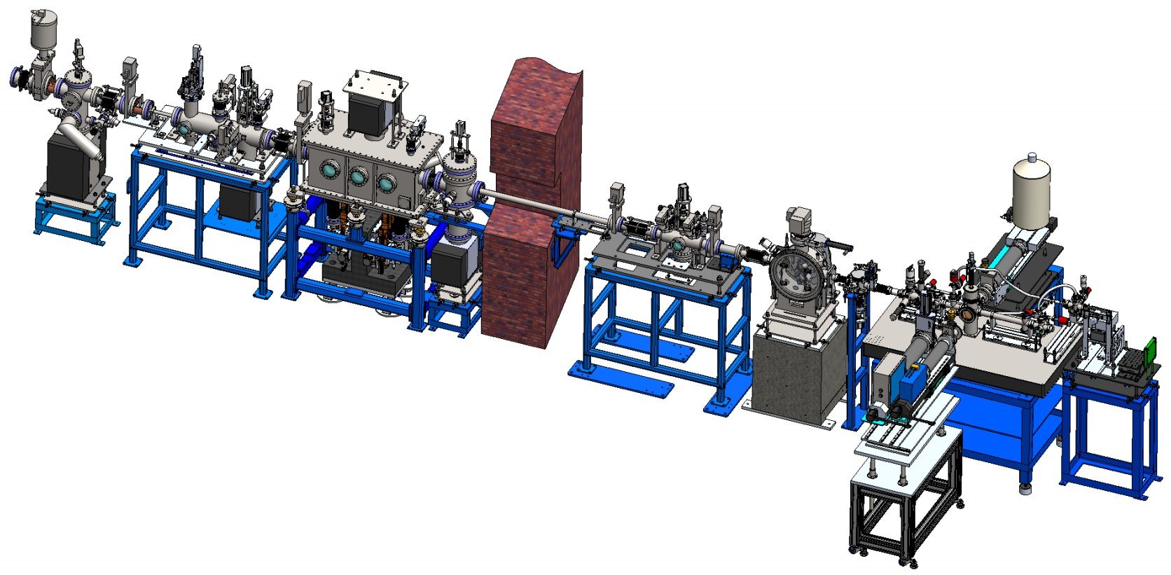
BL8 Optical Layout

Specification
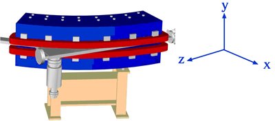
The CM system mainly consists of a rhodium-coated, single-crystal silicon flat mirror (Thales-SESO, France), a motorized bender (TOYAMA Co. LTD, Japan), five motorized stages (Oriental motor USA Corp., USA), a UHV chamber (SLRI, Thailand), and supporting granite. The size of mirror, 600 mm (length) × 50 mm (width) × 40 mm (height), is designed at an incident angle of 5 mrad for accepting most photons of 1 – 13 keV.
Table 1 Technical Specifications of XAS
X-ray source, optics, and upgraded specification of the beamline.
| Technique | X-ray absorption spectroscopy (XANES and EXAFS) |
|---|---|
| Energy range | 1 keV to 13 keV |
| Photon flux |
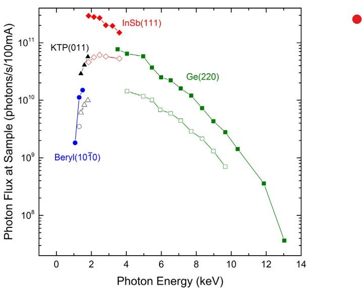
Maximum flux about 3 × 10¹¹ phs/s/100 mA is currently available for the Si, P, S, and Cl
K-edges. The lowest photon flux is 4 × 10⁷ phs/s/100 mA at the Pb L3-edge. |
| Beam size at sample |
Defocused (standard): 13 mm (h) × 1.5 mm (v) Focused down to 1 × 1 mm |
| X-ray source | 1.44 T Bending Magnet |
| Electron beam energy | 1.2 GeV |
| Electron beam current | 150 mA – 80 mA |
| Collimating mirror | Bendable, Rh-coated, single crystal silicon mirror |
| Monochromator | Fixed-exit double crystal monochromator |
Table 2 Technical Specifications of XFI
| Technique | X-ray Fluorescence Imaging |
|---|---|
| Energy excitation | 10 keV |
| Photon flux | 109 phs/s/100 mA |
| Detector | pnCCD with polycapillary optics |
| Image size at sample | 12.3 mm × 12.3 mm, 256 × 256 pixels |
| Spatial resolution | ~68 µm |
| Detection limit | 3.9 wt% (K) → 0.2 wt% (Zn) |
| X-ray source | 1.44 T Bending Magnet |
| Electron beam energy | 1.2 GeV |
| Electron beam current | 150 mA – 80 mA |
| Collimating mirror | Bendable, Rh-coated, single crystal silicon mirror |
| Monochromator | Fixed-exit double crystal monochromator |
Monochromator Crystals
| Crystal type | 2d spacing (Å) | Photon energy range (eV) | Measurable element |
|---|---|---|---|
| Beryl(10-10) | 7.98 | 1250 – 4780 | Mg |
| KTP(011) | 10.955 | 1250 – 4780 | Al |
| InSb(111) | 7.481 | 1830 – 7000 |
Si to Cl (K-edge) Rb to Cd (L3-edge) |
| Si(111) | 6.271 | 2180 – 8350 |
K (K-edge) In to Sb (L3-edge) |
| Ge(220) | 4.001 | 3440 – 13000 | Energy higher than 3.7 keV |