
Experimental-station
experimental-station
Beamline 3.2Ua/b · Photoemission Spectroscopy (PES) & PEEM
Experimental Station
Beamline Layout, Specification & Experimental Stations
Beamline Layout and Specification
Schematic of BL3.2U optical layout
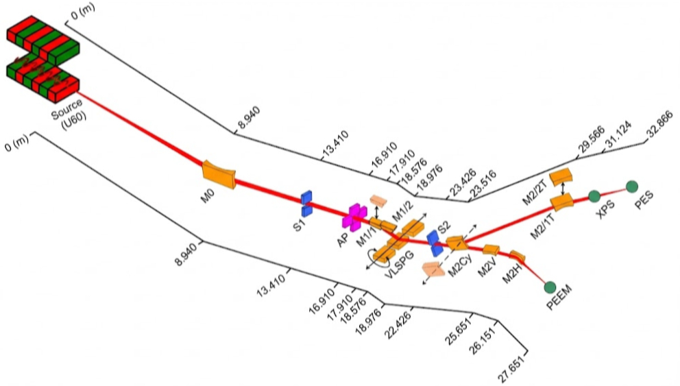

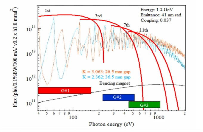
Source Description: The beamline utilizes a Planar Halbach-type Undulator manufactured by Danfysik. This insertion device features a pure permanent magnet (PPM) structure arranged in a planar Halbach configuration. By forcing the electron beam into a periodic sinusoidal trajectory, it generates high-intensity, nonpolarized synchrotron radiation. The photon energy is fully tunable by mechanically varying the undulator gap, providing a continuous spectrum of high-flux photons optimized for the soft X-ray and VUV regions.
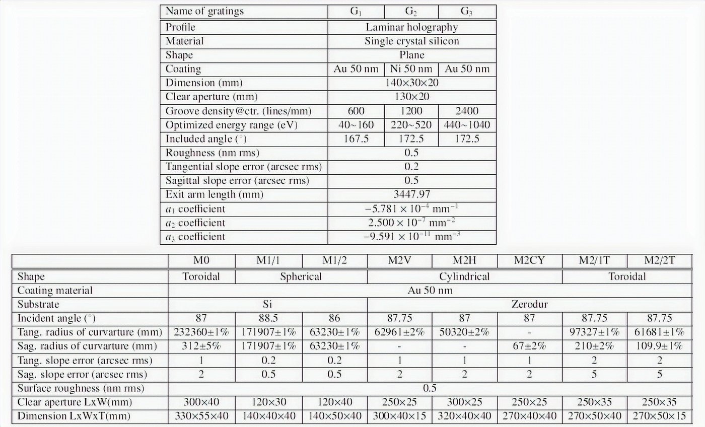
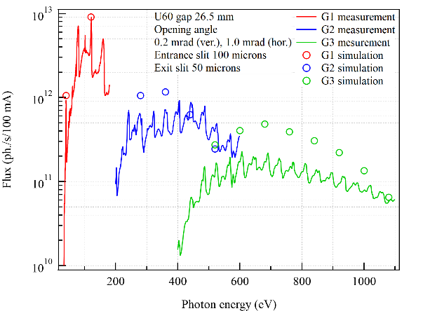
The Monochromator: The beamline employs a Varied Line Spacing Plane Grating (VLSPG) Monochromator manufactured by TOYAMA. This system features a set of three interchangeable Laminar Holographic Gratings on a single-crystal silicon substrate that can select a photon energy in the range 40-1040 eV. The beam passes through the entrance slit (S1) into VLSPG, producing a monochromatic beam that exits through the exit slit (S2). The entrance and exit slit can adjust a width in the range 0.05 to 0.5 mm, which has a direct effect on the beam spot size on the sample. The use of Laminar (rectangular) groove profiles effectively suppresses higher-order harmonic contamination, providing exceptional spectral purity for quantitative spectroscopy.
Specification Sheet of Optical System
Experimental Station
| Measurement Techniques |
|
|---|---|
| Applications | Surface-sensitive electronic structural investigation of materials |
| Radiation source | A planar Halbach-type undulator (Danfysik) |
| Magnetic field | 0.5467 T at 26.5 mm of gap |
| Period length | 60 mm |
| Number of periods | 41 |
| Total length | 2.460 m |
| Photon energy ranges | 40-160 eV and 220-1040 eV |
| Energy resolution | 0.1 meV at 10¹⁰ ph/s |
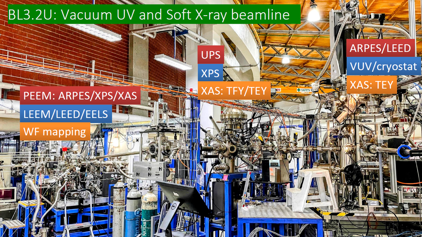
BL3.2Ua Photoemission Spectroscopy (PES)
Techniques using synchrotron radiation:
- Soft X-ray and VUV Angle-Resolved Photoemission Spectroscopy (ARPES)
- Soft X-ray and VUV Angle-Integrated and Angle-Resolved photoemission spectroscopy (SXPS, ARXPS, UPS)
- Soft X-ray absorption spectroscopy in the total electron yield mode (SXAS, NEXAFS)
Applications: Electronic structural investigation of materials
| Detectors (PES) | Scienta R4000 for ARPES, Thermo VG Scientific Alpha110 for UPS/XPS |
|---|---|
| Detectors (NEXAFS) | MCP for the total fluorescence yield mode, drain current for the total electron yield mode |
| Beam size (H x V) – simulation | 0.2 mm × 0.2 mm for XPS, NEXAFS and 0.3 mm × 0.1 mm at ARPES |
| Flux – simulation | 1.0×10¹⁰ phs/s at 100 mA at E/ΔE = 10,000 (emittance: 41 nm rad, energy spread: 0.0001) |
| Samples | Single crystal for ARPES, solid, powder, thin film, ultra-high vacuum compatible, and electrically conductive at the surface. |
| Sample environment |
|
ARPES End Station
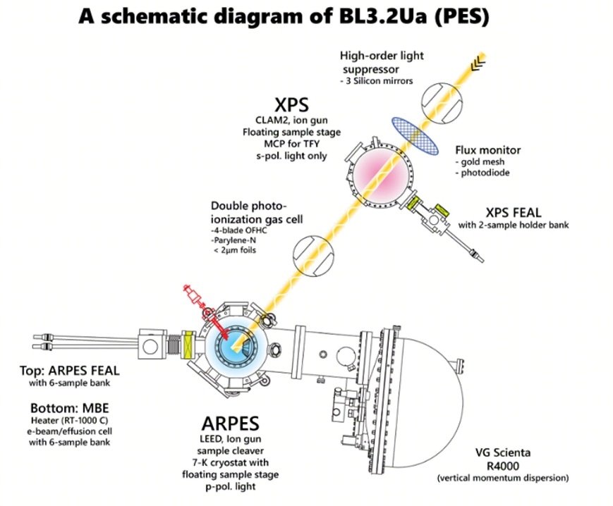
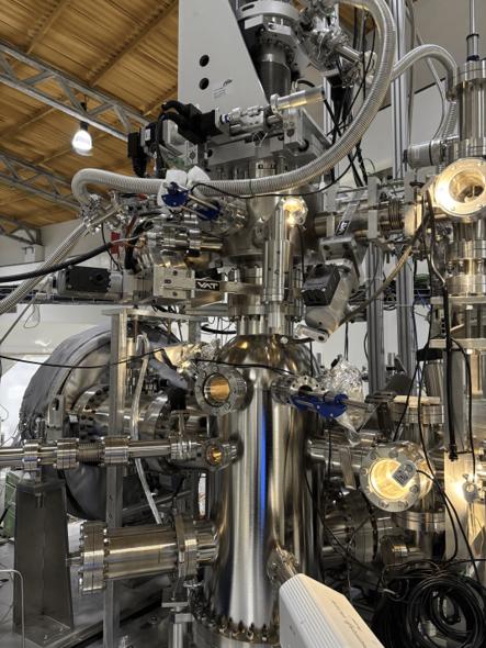
The ARPES end-station consists of photoelectron analysis, sample preparation, and 7 sample slots with linear sample transfer. An angle-resolved electron energy analyzer (VG Scienta, R4000) is installed in the photoelectron analysis chamber. The sample preparation can be carried out in the sample preparation chamber, located above the photoelectron analysis chamber, with the Ar ion sputtering gun (3 keV at ion energy), LEED optics (1 keV), alkali metal evaporator (K, Na, Li), and gas-inlet variable leak valves connected with the roughing pump. A sample can be handled on a 6-axis manipulator, and the temperature-controlled manipulator can be operated down to 8 K. A linear sample-transfer system transfers samples between the vacuum chambers without breaking UHV (~10⁻¹⁰ mbar at low temperature). The MBE chamber consists of a temperature-controlled sample manipulator (RT-1000K).
The Vacuum Ultraviolet (VUV) gas-discharged lamp system is available at the ARPES end station. Ultra-pure He (99.999%) gas is excited by high-intensity radio-frequency to generate 21.22 eV photon energy with high intensity (~10¹² photons/sec).
XPS End Station
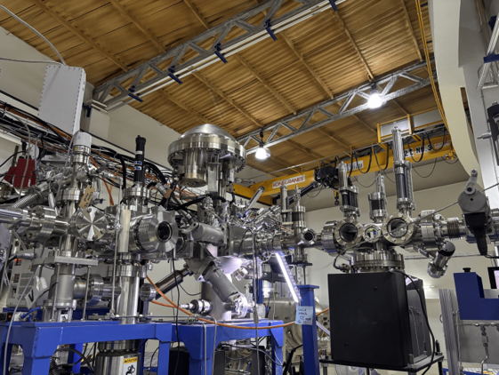
The XPS station performs at room temperature, and the system consists of the hemispherical electron Energy Analyzer (Alpha110) and an Ar ion sputtering gun (3 keV at ion energy). Samples are loaded into the UHV chamber (~10⁻¹⁰ mbar) by using the magnetic linear transfer rod from the first-entry air-lock system, pumped by the turbo-molecular pump, to the XPS analysis chamber, pumped by the 500 l/s ion and titanium sublimation pumps. The residual gas analyzer (100 atomic mass at maximum) is also available.
BL3.2Ub Photoemission Electron Microscopy (PEEM)
Techniques using synchrotron radiation: Photoemission Electron Microscopy (PEEM), micro/imaging-NEXAFS, XPS, ARPES, Work-Function mapping
Offline source: LEEM (IV), LEED (IV), and Micro EELS
Applications: Microscopy for surface, interface, and thin-film research. Electronic structural investigation of surface and interface materials.
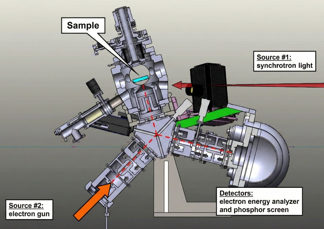
| Model | Elmitec PEEM III |
|---|---|
| Detectors | Micro-channel plate, Sensicam QE CCD camera (image resolution 30 nm) |
| Analyzer | Hemispherical electron energy analyzer |
| Sources | Synchrotron Radiation (Flux: 10¹² ph/s at 100 mA at 100 eV, Beam size: 0.2 x 0.1 mm²), Hg UV lamp, electron gun for low-energy electron microscopy (LEEM) |
| Samples | Must be flat and smooth, ultra-high vacuum compatible, and electrically conductive. Non-conductive samples can be coated with metal films before imaging. |
| Sample environment |
|
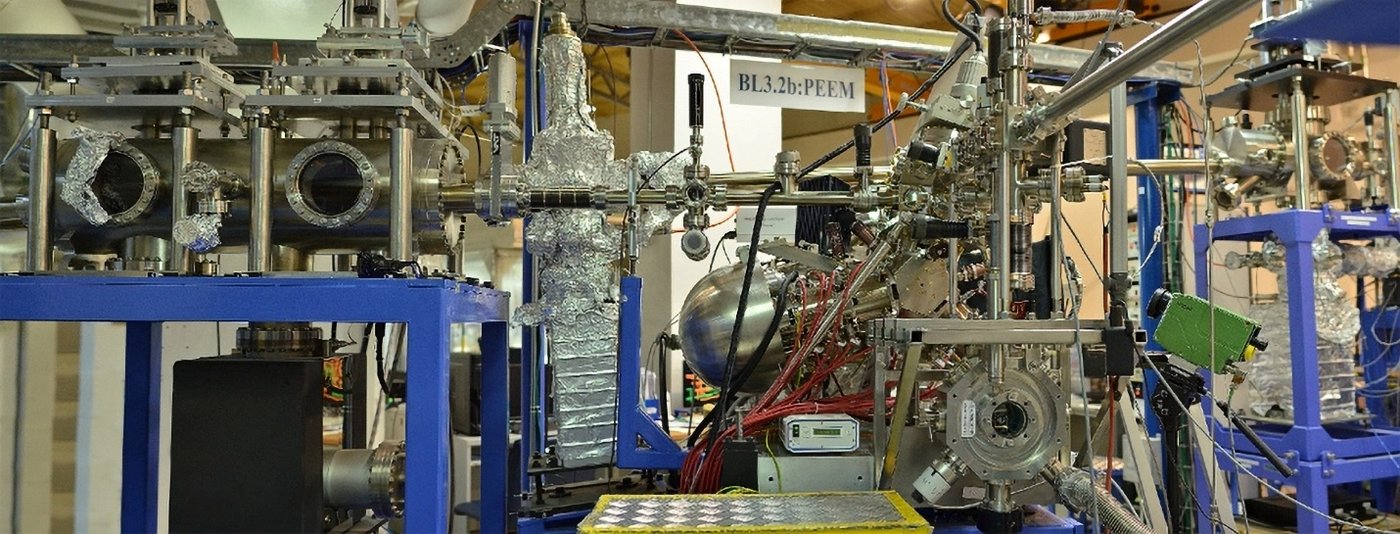
PEEM End Station
At PEEM station, a sample is irradiated with monochromatic light from a varied line-spacing plane-grating monochromator. Electrons, created by photoemission and photoabsorption processes, are projected by a set of magnetic lenses onto a micro-channelplate intensifier and a phosphor screen, where the final image forms. By scanning incident photon energy and capturing PEEM image at each energy step, a series of images that contain photoabsorption spectra from nanometer-sized areas of the sample can be obtained. Alternatively, the photon energy is fixed, and an electron energy analyzer is used to determine the photoemission spectrum of photoelectrons emitted from specific areas of the sample.
The electron gun enables structural characterization of crystalline surfaces through Low Energy Electron Microscopy (LEEM), which is highly sensitive to surface topography, atomic step edges, and surface termination. LEEM is typically used to monitor real-time thin-film growth, structural domain formation, gas adsorption, and phase transitions. In reciprocal space mode, the electron gun allows Micro Low-Energy Electron Diffraction (μ-LEED) from regions as small as 0.5 mm using an illumination aperture. By scanning the incident electron energy, LEED intensity curves can be efficiently recorded. It is also possible to select an off-normal LEED spot to form LEEM images in dark-field mode, thereby enhancing contrast between structural islands.